Measurement Technology Group
Optical interferometry as a measurement tool in nano-technology
The measurement technology group headed by Prof. Peter Lehmann, who joined CINSaT in 2017, belongs to the department of electrical engineering and computer science. Hence, the research work focuses on the use of electronic or optoelectronic components and the development of appropriate methods, mainly interferometric techniques, to measure 3D surface structures and distance changes. Optical interferometry is one of the most fascinating measuring principles as it easily achieves a resolution below one nanometer in the axial direction and, therefore, shows a wide range of applications in industry and research.
However, the lateral resolution and the three-dimensional measurement capabilities of optical interference microscopes suffer from the diffraction limit. Hence, it is a big challenge to understand the limiting phenomena in detail and search for options that improve instruments with respect to their lateral resolution capabilities. In this context, the measurement technology group could gain some progress in recent years.
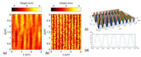
With a self-constructed high-resolution Linnik interference microscope a strong relationship between the wavelength used to determine the phase of an interference signal and the lateral resolution limit could be established. The so-called NA-effect provides wavelength contributions to an interference signal that are far above the maximum wavelength of the light source’s wavelength spectrum. Phase analysis at these wavelengths improves the lateral resolution of an interference microscope significantly as it is illustrated in Fig. 1 by example of a Blu-ray disc structure.
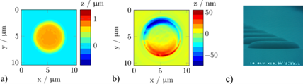
The same instrument enabled the development of a novel measurement strategy that might be useful for a fast inspection of micro- and nano-particles: Putting a master particle as a reference object instead of a plane mirror into the reference arm of the interferometer provides a direct optical comparison of the particle under investigation and the master particle. Due to similar optical and geometrical properties of the measurement and the reference object (similar slope angles, shape, size, and reflection coefficient) improved measurement capabilities (e.g. maximum measurable slope angle) could be achieved. This was verified in a joint research project with the technological electronics group (Prof. H. Hillmer). Measurement results for a micro-particle produced by nanoimprint-lithography are shown in Fig. 2.
Interferometric topography sensors are known as very sensitive to vibration since several camera frames have to be taken for a 3D surface reconstruction, which sometimes contradicts demands of practical applications. A new approach to overcome these problems uses an interferometer with a RGB-camera and an oscillating reference mirror. The surface structure is reconstructed from two subsequent RGB images using a quadrature-based phase retrieval algorithm as it is demonstrated by Schake et al. (2019). Additionally, this approach paves the way to dynamic measurements.
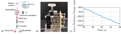
Further, fiber-coupled micro-optical interferometers represent very interesting devices, as they are fast and accurate. Therefore, they may substitute tactile stylus sensors in certain applications (Hagemeier et al. (2019)). Due to their sensitivity to single atomic layers and their high data rate they enable dynamic measurements of distance changes, e.g. in order to monitor evaporation processes as shown in Fig. 3. Sensors for different applications following the working principle of sinusoidal phase modulation have been tested successfully in recent years.
References
Lehmann et al. (2018) P. Lehmann, W. Xie, B. Allendorf, S. Tereschenko, Opt. Exp. 26, 7376-7389, (2018)
Allendorf et al. (2019) B. Allendorf, E. Käkel, Uh-Myong Ha, S. Hagemeier, H. Hillmer, P. Lehmann,
Opt. Lett. 44, 3550-3553 (2019)
Schake et al. (2019) M. Schake, P. Lehmann, Opt. Exp. 27, 16343-16358 (2019)
Hagemeier et al. (2019) S. Hagemeier, S. Tereschenko, P. Lehmann, Technisches Messen 86, 164-174 (2019)
Prof. Dr. Peter Lehmann
full member

- Location
- Universität Kassel
Fachbereich 16 - Elektrotechnik & Informatik
Wilhelmshöher Allee 71
34121 Kassel
- Room
- 3121