Technological Physics: Nano Diamond Group
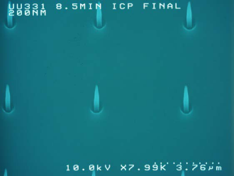
Diamond is a material with excellent properties due to its structure and composition. Its face-centered cubic crystal lattice is a perfect host of different defect centers, so-called color centers, whose properties, especially the capability of emitting single photons, can serve in quantum information technologies (QIT). As a high refractive index material only a small part of the photons emitted by these color centers in diamond can be collected. To enhance the photon collection efficiency photonic structures, such as photonic crystals, nanopillars, waveguides, etc., are necessary. The group is fabricating such structures by top-down or bottom-up techniques. Diamond nanopillars with diameters between 1 µm and 50 nm were prepared by electron beam lithography (EBL) and subsequent inductively coupled plasma reactive ion etching (ICP-RIE) with oxygen plasma (Fig. 1 (a)). Nitrogen-vacancy (NV) color centers were incorporated in the monocrystalline diamond samples before structuring (Fig. 1 (b)). By overgrowth of diamond nanopillars in presence of Si source silicon-vacancy (SiV) centers were integrated into the structures. When monocrystalline diamond pillars with top diameters of 30 nm were overgrown, arrays of nanopyramids were obtained due to the different growth rates in different crystallographic directions (Fig. 1 (c)). In all cases an enhance intensity of the light emission for the nanostructures was observed (Fig. 1 (d)).
(Kopie 5)
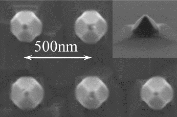
Fig. 1. Monocrystalline diamond nanopillars (a) with integrated NV centers (b); monocrystalline diamond nanopyramids (c) with integrated SiV centers (d).
In addition, photonic crystals were prepared in nanocrystalline diamond (NCD) membranes from films deposited on Si wafers coated with a sacrificial SiO2 layer. The design included air holes with a diameter of 230 nm and a period of 300 nm (Fig. 2 (a)). The fabrication of the photonic crystals includes their definition by EBL and RIE with O2 plasma, followed by wet chemical etching of the sacrificial SO2 layer. The obtained photonic structures possessed holes with vertical and smooth walls (Fig. 2 (b)). The fabrication and investigation of diverse diamond photonic structures is currently financially supported by the German Ministry of Education and Research (BMBF).

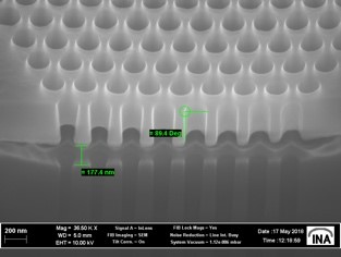
Fig. 2. Photonic crystal structures based on NCD membrane: (a) top view and (b) cross section.
Solid state implementations of qubits are considered to be advantageous for diverse applications. Individual qubits may be generated and controlled employing the NV color centers in diamond. This exceptionally convenient quantum system operating even at room temperature can be optically initialized, read out and manipulated with microwaves. Long spin coherence times can be achieved by swapping the NV qubit state onto that of a nuclear spin qubit placed nearby. For long distance entanglement the SiV centers can be employed as qubits. A project together with the groups of Prof. C. Koch and Prof. K. Singer, as well as partners from Mainz and Stuttgart, funded by Volkswagen Foundation aims at the prototypical implementation of diamond structures integrated with color centers as quantum money and nano sensors. The quantum money will represent arrays of diamond nanopillars which will be implanted with single N ions (Fig. 3 (a) and (b)). As nano sensors AFM tips and needles with NV centers in the apex will be applied (Fig. 3 (c) and (d)). The technology development for both types of diamond nanostructures is in progress.
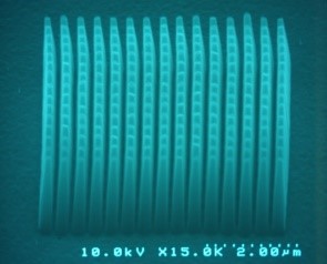
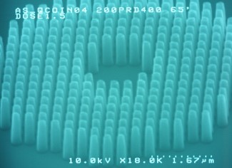
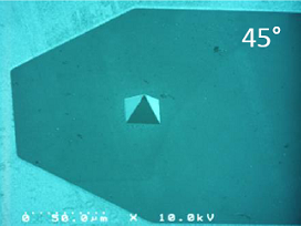
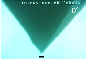
Fig. 3. SEM images of arrays of diamond nanopillars (a), (b) and of diamond AFM tips (c), (d).
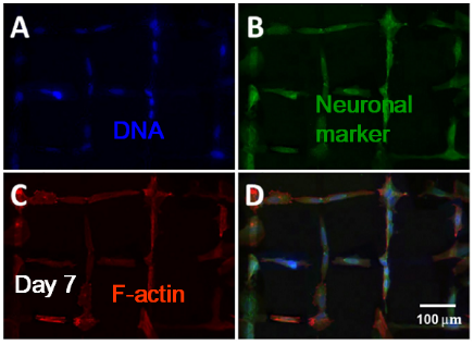
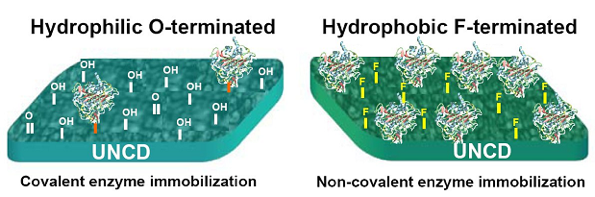
The focus of the collaboration with several groups from the Institute of Biology (Prof. M. Stengl, Prof. F. Herberg) was set on the preparation and application of diamond platforms for attachment of neurons and immobilization of proteins. An enhanced attachment of the neurons, especially on the modified hydrophilic ultrananocrystalline (UNCD) surfaces was established. It was especially advantageous for the immunocytochemical procedures with the cell cultures where the cell losses during washing steps were significantly reduced by one order of magnitude in comparison to the controls. The patterning of the surface termination (hydrophilic – hydrophobic) resulted in preferential attachment and growth of cells on the hydrophilic grid (Fig. 4 (a)). Furthermore, the different surface terminations of UNCD can be applied for realization of different approaches for immobilization of proteins (Fig. 4 (b)). The initial results will be implemented in the frame of Graduate School “Biological Clocks” for the realization of bio-sensors for biochemical measurements of time-resolved cell signaling.

(a)
(b)
Fig. 4. Patterned termination of UNCD surface (in this case with O- and F- termination) leading to directional attachment and growth of neurons (a); Different approaches (covalent and non-covalent) applied for the immobilization of proteins depending on the surface modification.
apl. Prof. Dr. Cyril Popov
full member
- Telephone
- +49 561 804-4205
- popov[at]ina.uni-kassel[dot]de
- Location
- Universität Kassel
Fachbereich 10 - Naturwissenschaften & Mathematik
Institut für Nanostrukturtechnologie und Analytik
Heinrich-Plett-Str. 40
34132 Kassel
- Room
- 2115