Equipment
Cleanroom Equipment
On this page you find an overview of all machines which are available at INA. If there are questions please do not hesitate to contact us.
Lithography
Zeiss NVision 40 High End Cross Beam
- Electron column: high resolution (1,3 nm) field emission
- Ion column: high resolution (4 nm), suitable for deposition (local microdeposition) and etching
![[Translate to English:] Foto: Zeiss NVision 40 High End Cross Beam](/forschung/files/INA/Technische-Elektronik/Ausstattung/Fotos/pool_zeiss_nvision_40.jpg)
Karl Süss MA6 Maskaligner
- NanoImprint with SCIL Tooling for hybride Stamps
- up to 6“-substrates, up to 7“-masks
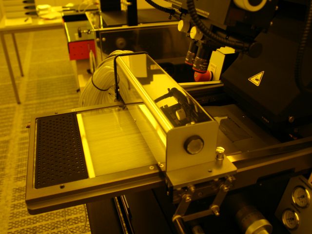
Karl Süss MA4 Maskaligner
- up to 4“-substrates, up to 7“-masks
- Resolution: standard 800 nm, optional up to 300 nm
![[Translate to English:] Foto: Karl Süss MA4 Maskaligner](/forschung/files/INA/Technische-Elektronik/Ausstattung/Fotos/pool_suess_ma4.jpg)
EVG Al-4 Maskaligner
- up to 4“-substrates, up to 5“-masks
![[Translate to English:] Foto: EVG Al-4 Maskaligner](/forschung/files/INA/Technische-Elektronik/Ausstattung/Fotos/pool_evg_al4.jpg)
Raith eLine Electron Beam Lithography
- High resolution (20 nm and below)
- 100 x 100 mm laser interferometer table
- Positioning accuracy 2 nm in x- and y-direction
![[Translate to English:] Foto: Raith eLine Elektronenstrahlithografie](/forschung/files/INA/Technische-Elektronik/Ausstattung/Fotos/pool_raith_eline.jpg)
Deposition
Roth & Rau Ionsys 1000 IBD
Ion Beam Deposition
- Class 1 cleanroom section
- Multilayer systems (DBR, VCSEL etc.)
- In-situ process control
- Material: metals (e.g. Al, Zr, Cr), oxides (e.g. ITO, TiO, SiO2), nitrides (e.g. SiN)
- Process gases: Argon (Ar), Xenon (Xe), Oxigen (O2), Nitrogen (N2
- Prozessgase: Argon (Ar), Xenon (Xe), Sauerstoff (O2), Stickstoff (N2)
![[Translate to English:] Foto: Roth & Rau Ionsys 1000 IBD](/forschung/files/INA/Technische-Elektronik/Ausstattung/Fotos/pool_ionsys_1000.jpg)
Pfeiffer PLS 500 Evaporation System
- Thermal or electron beam
- Material: Titanium (Ti), Nickel (Ni), Chromium (Cr), Platinum (Pt), Aluminium (Al)
![[Translate to English:] Foto: Pfeiffer PLS 500 Aufdampfanlage](/forschung/files/INA/Technische-Elektronik/Ausstattung/Fotos/pool_pls_500.jpg)
Balzers BAK 600 Evaporation System
- Thermal or electron beam
- Process gas: Argon (Ar)
- Material: Nickel (Ni), Titanium (Ti), Platinum (Pt), Gold (Au), Germanium (Ge), Chromium (Cr)
![[Translate to English:] Foto: Balzers BAK 600 Aufdampfanlage](/forschung/files/INA/Technische-Elektronik/Ausstattung/Fotos/pool_bak_600.jpg)
Phönix Evaporation System (self made)
- Thermal
- Material: Zinc (Zn), Gold (Au)
![[Translate to English:] Foto: Phönix Aufdampfanlage](/forschung/files/INA/Technische-Elektronik/Ausstattung/Fotos/pool_phoenix.jpg)
Oxford Plasmalab 80 PECVD
Plasma Enhanced Chemical Vapour Deposition
- Process gases: Silan (SiH4), Hydrogen (H2), Ammonia (NH3), Nitrous oxide (N2O)
- Material: Silicon Nitride (SiN), Silicon Oxide (SiO), Silicon (Si)
![[Translate to English:] Foto: Oxford Plasmalab 80 PECVD](/forschung/files/INA/Technische-Elektronik/Ausstattung/Fotos/pool_plasmalab_80_pecvd.jpg)
Zeiss NVision 40 High End Cross Beam
- Electron column: high resolution (1,3 nm) field emission
- Ion column: high resolution (4 nm), suitable for deposition (local microdeposition) and etching
Dry Etching
Castor and Pollux RIE
Reactive Ion Etching
Parallel Plate Reactor
- Process gases: Argon (Ar), Trifluoromethane (CHF3), Sulfur hexafluoride (SF6), Oxygen (O2)
- Material: Silicon Nitride (SiN), Silicon Oxide (SiO)
![[Translate to English:] Foto: Castor und Pollux RIE](/forschung/files/INA/Technische-Elektronik/Ausstattung/Fotos/pool_castor_pollux.jpg)
(Kopie 16)
Oxford Plasmalab 80 Plus RIE
Reactive Ion Etching
Parallel Plate Reactor
- Process gases: Hydrogen (H2), Methan (CH4)
- Material: Indium (In), Phosphorus (P), Gallium (Ga), Arsenic (As) compound semiconductors (e.g. InP)
![[Translate to English:] Foto: Oxford Plasmalab 80 Plus RIE](/forschung/files/INA/Technische-Elektronik/Ausstattung/Fotos/pool_oxford-plasma.jpg)
2 Oxford Plasmalab 100 ICP-RIE
Inductive Coupled Plasma - Reactive Ion Etching
- ICP 1: for deep etching of silicon with flourine-donators (Bosch-process)
- ICP2: for etching of semiconductor materials (e.g. GaAs) with chlorine-donators
![[Translate to English:] Foto: Oxford Plasmalab 100 ICP-RIE](/forschung/files/INA/Technische-Elektronik/Ausstattung/Fotos/pool_plasmalab100icp.jpg)
TePla 200-G Oxygen Asher
- Etching of photo resist and organic residues
- Process gas: Oxygen (O2)
![[Translate to English:] Foto: TePla 200-G Plasmaverascher](/forschung/files/INA/Technische-Elektronik/Ausstattung/Fotos/pool_tepla200-g.jpg)
diener electronic NANO Oxygen Asher
- Etching of photo resist and organic residues
- Active Cooling, Optical Endpoint Detection
- Process gas: Oxygen (O2), Argon (Ar)
- Power: 600 W
![[Translate to English:] Foto: diener electronic NANO Plasmaverascher](/forschung/files/INA/Technische-Elektronik/Ausstattung/Fotos/pool_diener_nano.jpg)
Further Equipment
Bal-Tec CPD 030 Critical Point Dryer
- Process gas: Carbon Dioxide (CO2)
![[Translate to English:] Foto: Bal-Tec CPD 030 Kritisch-Punkt-Trockner](/forschung/files/INA/Technische-Elektronik/Ausstattung/Fotos/pool_bal-tec_cpd_300.jpg)
Xerion RTA
Rapid Thermal Annealing
- Process gas: Argon (Ar)
- Temperatures up to 400°C
![[Translate to English:] Foto: Xerion RTA](/forschung/files/INA/Technische-Elektronik/Ausstattung/Fotos/pool_xerion_ofen.jpg)
Analytics
Zeiss NVision 40 High End Cross Beam
- Electron column: high resolution (1,3 nm) field emission
- Ion column: high resolution (4 nm), suitable for deposition (local microdeposition) and etching
Zygo NewView 5000 White Light Interferometer
- Vertical Resolution up to 0.1nm
- Objectives: 5x Michelson, 50x Mirau
- xy motordesk for stitching
- Extended vertical scan length up to 20mm
![[Translate to English:] Foto: Zygo 5000 Weißlichtinterferometer](/forschung/files/INA/Technische-Elektronik/Ausstattung/Fotos/pool_zygo.jpg)
Leica DMR Microskope
- up to 1000x Magnification
- Contrast method: bright field, dark field, differential interference contrast
- Impinging light and transmitted light
![[Translate to English:] Foto: Leica DMR Mikroskop](/forschung/files/INA/Technische-Elektronik/Ausstattung/Fotos/pool_leica_drm.jpg)
SENTECH SENpro Spectroscopic Ellipsometer
- Monitoring of film thickness
- Wavelength range: 350 nm - 1050 nm
![[Translate to English:] Foto: SENTECH SENpro Ellipsometer](/forschung/files/INA/Technische-Elektronik/Ausstattung/Fotos/pool_sentech.JPG)
Plasmos SD-2100 Ellipsometer
- Monitoring of film thickness
![[Translate to English:] Foto: Plasmos SD-2100 Ellipsometer](/forschung/files/INA/Technische-Elektronik/Ausstattung/Fotos/pool_plasmos_sd2100.jpg)
Ambios Technology Oberflächenprofilometer XP-100
- 3 nm resolution
- 0,03 - 10 mg stylus force
- 1,2 mm max. masurement range in z-direction
- analysis of step hights , layer ticknesses, roughness, ripples, thin layer stress
![[Translate to English:] Foto: Ambios Technology Oberflächenprofilometer XP-100](/forschung/files/INA/Technische-Elektronik/Ausstattung/Fotos/pool_ambios_profilometer.jpg)
Sloan Dektak IIA Profilometer
- 20 nm resolution
![[Translate to English:] Foto: Sloan Dektak IIA Profilometer](/forschung/files/INA/Technische-Elektronik/Ausstattung/Fotos/pool_sloan_dektak.jpg)
Rohde & Schwarz Spectrum Analyzer FSB
- Band width: 9 kHz-30 GHz
![[Translate to English:] Foto: Rohde & Schwarz Spektrumanalysator FSB](/forschung/files/INA/Technische-Elektronik/Ausstattung/Fotos/pool_rohde_schwarz_fsp.jpg)
Agilent 86142 B Optical Spectrum Analyzer
- Band width: 600-1700 nm
![[Translate to English:] Foto: Agilent 86142 B Optischer Spektrumanalysator](/forschung/files/INA/Technische-Elektronik/Ausstattung/Fotos/pool_agilent_86142.jpg)