High Resolution 3D NanoImprint Stamps and NanoImprint Technologies
General Information
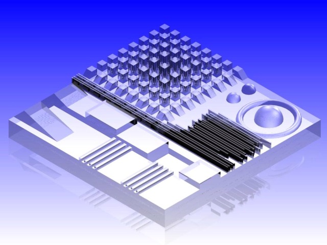
NanoImprint is a molding process, in which nanostructures are transferred from a stamp (negative) to curable materials (positive). There is not only the possibility of molding a large number of nanostructure systems, but also manufacturing high-precision nanostructures on larger areas by means of a “Step-and-repeat” or a “Roll”-process. NanoImprint is not only interesting for functional surfaces and nano-optics, but also on the roadmap to future chip fabrication from 2020. Hence, this specific type of nano-technology manifests its extraordinarily braid field of application as well as a distinct future perspective and sustainability. A consortium of institutes of the University of Kassel, the Photonik Zentrum Hessen in Wetzlar and the University of Applied Sciences Giessen-Friedberg contributes expertise from fundamental methods to the actual implementation of the technology. A novel nanotechnological fabrication method for high-precision 3D-NanoImprint-stamps, which was developed and tested at INA and applied for a patent 2006, provides a valuable base and an essential unique selling proposition.
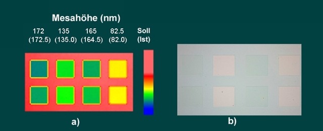
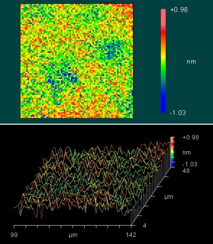
In the first quarter of 2008 INA succeeded in the fabrication of structures with a vertical resolution of only 0.1nm. This big step finally allows the fabrication of complex 3D-structures with very high vertical resolution by means of molding techniques for the very first time. Figure 2 and Figure 3 show characterizing measurements of the surface properties of the stamp and the resulting molded structures. In this example the novel stamp shows its enormous potential of reliable reproduction of extreme surface flatness of molded structures (approx. 0.2 nm). It is to be pointed out that the same planarity is reached also on adjacent surfaces in a different vertical position. Similarly to a topographic map, the different colors indicate the topography of the molded structures.
In its research, the NanoImprint Consortium Hessen takes advantage of synergetic effects of the diverse expertise of the disciplines biology, chemistry, electrical engineering and physics.The fabrication of the high-resolution stamp should be enhanced by an anti-adhesion-coating. Applications of the methodology will be executed in the following fields: organic LEDs, organic electronics, inorganic/organic Hybrid-Laser, biomedical Nanospectrometer, quantum dot structures for the high bit-rate communication, biosensor technology, Microfluidics, magnetic memory structures, optical ASICs, secure optical sensor technology, light channeling (hessen-nanotech NEWS / DBU) and Nanoantennas-Arrays. For this reason, these projects incorporate also homogenously into the focus topic “nanophotonics” of the nano network in Hessen, as well as into the topic of Network of Competence for Optical Technologies Hesse/Rhineland-Palatinate – Optence.
Partners in the NanoImprint Consortium Hessen
The following partners cooperate in NanoImprint Consortium Hessen:
- Prof. Dr.-Ing J. Börcsök, the Chair for Computer Architecture and System Programming
- Prof. Dr.-Sc.Tech. D. Dahlhaus, Communications Laboratory
- Prof. Dr. rer.nat. A. Ehresmann, Thin Layers Physics
- Prof. Dr.rer.nat. F. Herberg, Department of Biochemistry
- Prof. Dr. rer.nat. H. Hillmer, INA, Technological Electronics Group
- Dr.-Ing. Lauinger, PZH
- Prof. Dr. rer.nat. J.-P. Reithmaier, INA, Technological Physics Group
- Prof. Dr.-Ing. U. Ricklefs, Competence Center of Nanotechnology and Photonics
- Prof. Dr. rer.nat. J. Salbeck, Macromolecular Chemistry and Molecular Materials Group
- Dr. rer.nat. T. Schanze, PZH
- Prof. Dr. rer.nat. U. Siemeling, Institute of Chemistry
- Prof. Dr. rer.nat. T. Tschudi, PZH
Industry Cooperation in the Field of NanoImprint and High Resolution 3D-NanoImprint-Templates
In the NanoImprint Consortium Hessen institutes of the University of Kassel, the Photonik Zentrum Hessen (PZH) and the University of Applied Sciences Giessen-Friedberg cooperate with the following companies: BBraun, Carl Zeiss, SüssMicrotech, Corrsys 3D, HIMA, Vistec, Opsolution, AMO, Laytec, MaZet and others. In this case, the nanoimpront-technology is explicitly used for the following reasons: It offers precision in the sub nanometer region, it can be used to fabricate 3D-nanostructures even on large areas, it addresses the mass market, requires mostly low cost organic material and has the potential of providing relatively low cost fabrication capabilities at high output rates. Its magic formula is the definite return of the high investment in a stamp by cheap and highly precise production of a high number of nanostructures.