Pronano
Technology for the Production of Massively Parallel Intelligent Cantilever Probe Platforms for Nanoscale Analysis and Synthesis
Scanning proximity probes (SPP) are uniquely powerful tools for analysis, manipulation and bottom-up synthesis: they are capable of addressing and engineering surfaces at the atomic level and are the key to unlocking the full potential of Nanotechnology.
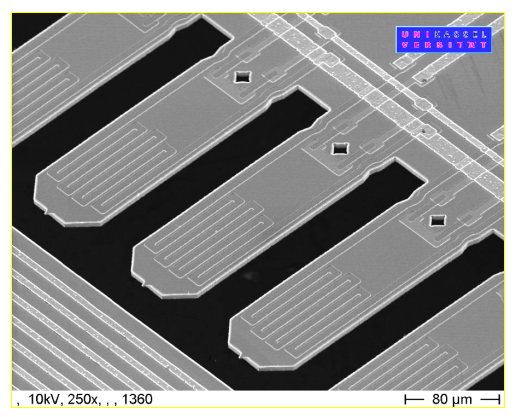
Current SPP nanotools are limited to single probes with pitifully slow processing rates and, even at the research level, attempts at multiprobe systems have achieved only a 32 x 32 array. This could be a terminal limitation for the future of Nanotechnology, in particular for bottom-up manufacturing, with little prospect for economic throughputs, unless 2-dimensional massively parallel probe arrays can be realised.
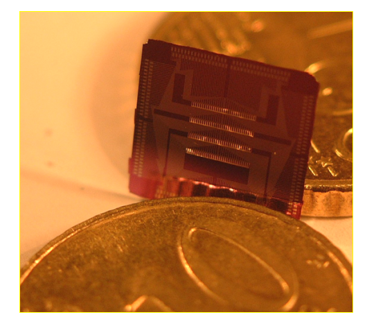
Such a development would revolutionise Nanotechnology, triggering an avalanche of new products and processes in a wide range of applications including surface chemistry, materials and the life-health industries. This ground-breaking technology development is the ambitious principal aim of this proposal. Generic massively parallel intelligent cantilever-probe platforms will be produced through a number of existing and ground-breaking techniques. The ultimate product will be a packaged VLSI NEMS-chip (Very Large Scale Integrated Nano Electro Mechanical System) incorporating 128x128 proximal probes, fully addressable with control and readout interconnects and advanced software.
To validate this novel technology, a series of demonstrations are planned where relevant SMEs will use this technology to carry out sub-10 nm metrology for high throughput manufacturing. Furthermore selected key applications and the results will be used to educate and inform in support of the development of new nanotechnology processes and products. It is the aim of PRONANO that the new massively parallel scanning probe nanotools with VLSI ASNEMS (application specific nanoelectromechanical systems) chips inside should empower nanotechnologists and drive the rapid development of nanoscience, leading to new nanotechnology processes and their industrial exploitation. They will secure the future of nanotechnology with economic throughputs leading to new manufacturing industries.
Project Participants:
- Nanoworld Services GmbH, Erlangen, Germany ( Coordinator )
- TU Ilmenau, Ilmenau, Germany ( Vice Coordinator )
- INA University of Kassel, Kassel, Germany
- Profactor Produktionsforschungs GmbH, Seibersdorf, Austria
- Uppsala University, Uppsala, Sweden
- NaWoTec GmbH, Rossdorf, Germany
- Wroclaw University of Technology, Wroclaw, Poland
- Infineon Technologies AG, Munich, Germany
- CLRC Rutherford Appleton Laboratory, Oxfordshire, United Kingdom
- Slovak Academy of Sciences, Bratislava, Slovakia
- FSRM, Neuchatel, Switzerland
- Inst. Nat. Polytechnique de Lorraine, Nancy, France
- Microsystems Ltd., Varna, Bulgaria
- ID-MOS SA, Gradignan, France
- Forschungszentrum Dresden-Rossendorf, Dresden, Germany
- Vistec Semiconductor Systems GmbH, Weilburg , Germany
- SIOS Messtechnik GmbH, Ilmenau, Germany