Interview: How quantum dots can reduce the ecological footprint
Prof. Dr. Johann-Peter Reithmaier
As part of BiTWerk, we at the Department of Technical Physics always aim to use our research to help minimize the impact of manufacturing technologies and materials on the environment and thus the ecological footprint.
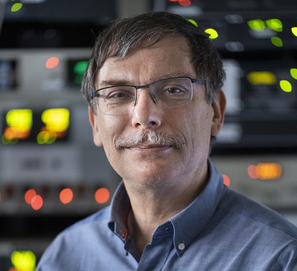
Interview with Prof. Dr. Johann-Peter Reithmaier, Head of Technical Physics, Director of the Institute for Nanostructure Technology and Analytics (INA) and Spokesperson of the Center for Interdisciplinary Nanostructure Science and Technology (CINSaT) at the University of Kassel, Dr.-Michael Hartung, Head of the Application Center UNIfipp (function-integrating polymer processing) and M.Sc. Matthias Koch, Head of the project "CoSoWin - Windows with integrated solar cells based on Luminescent Solar Concentrator (LSC) technology for energy supply", both from the Department of Polymer Engineering headed by Prof. Dr.-Ing.
- The Nobel Prizes in Chemistry were awarded on October 4, 2023. The three nanoscientists Moungi G. Bawendi, Louis E. Brus and Alexei I. Ekimov "for the discovery and synthesis of quantum dots". Quantum dots are also produced and studied in physics. Prof. Dr. Reithmaier, you are renowned in Germany and beyond for this field of research. Where were you when you heard about the scientists' award and what was going through your mind?
Prof. Dr. J.-P. Reithmaier: We had an external group seminar when I had already been informed of the award winners via an e-mail request from dpa before the announcement. There were probably already some leaks. Unfortunately, I didn't have time to reply at such short notice. Of course, I was very happy for my colleagues from chemistry. The research field of quantum dots is very broad. You can see that from the fact that I am a physicist and the quantum dots that we generate and study here in the department actually differ significantly in size, production and application from those for which the Nobel Prize winners were awarded. Quantum dots generally consist of 10,000 to 1,000,000 atoms of a semiconductor material and are only a few nanometers in size. The special thing about all quantum dots is that their ability to generate light and thereby reproduce the entire color spectrum can be used depending on their size. This determines the emission properties, i.e. the wavelengths that the particles emit and therefore also the coloration. Previously, colors could only be achieved through the chemical composition of different materials.
- What approach do you take as a quantum physicist and how do the quantum dots in nanophysics differ from those in chemistry?
Prof. Dr. J.-P. Reithmaier: The quantum dots developed by chemists and synthesized from a solution can be used in the screens of televisions, PCs or cell phones, for example. They absorb light and emit it again. This results in a much wider beam angle, which improves the color fidelity and brilliance of the screen. These quantum dots emit light spectra that we can see. The quantum dots that we generate in nanophysics using a deposition process during the production of crystalline materials have different material compositions and emit at longer wavelengths. Visible light is between 400 and 800 nanometers in wavelength and we are at around 1300 to 1500 nanometers with our quantum dots. This may be visible to some insects and reptiles, but not to us. These quantum dots are used to transmit information. This is where we are in optoelectronics. So if you have a high-resolution screen, for example, you need a lot of information for the display. Just like a telephone call or an e-mail, this information is transmitted optically via optical fiber. For this transmission, you need a semiconductor laser and a detector that emits and collects the light. This is converted into electrical signals which can then be seen on the screen, TV or PC. These could be images or videos, but also text or any other large amount of data.
- What role do quantum dots play in this?
Prof. Dr. J.-P. Reithmaier: The quantum dots are the decisive material, because they define the light emission when positive and negative charge carriers react with each other. Each quantum dot emits a light quantum (photon) at the same time and with billions of quantum dots, a lot of light is produced. The more quantum dots I have, the more photons I generate within a certain volume and within a certain period of time. Quantum dots enable the semiconductor lasers produced to work more efficiently, i.e. the transformation from electrical to optical energy is more efficient compared to previous processes. In general, optical processes can be used to transmit much larger amounts of data compared to electrical signals. Using this technology, up to 20 terrabits per second of data can now be transmitted via a single optical fiber. This is equivalent to broadcasting around 1,000,000 TV channels simultaneously.
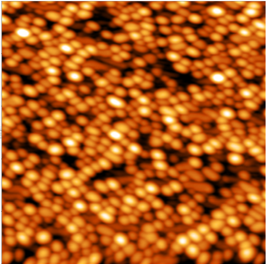 Image: Technische Physik
 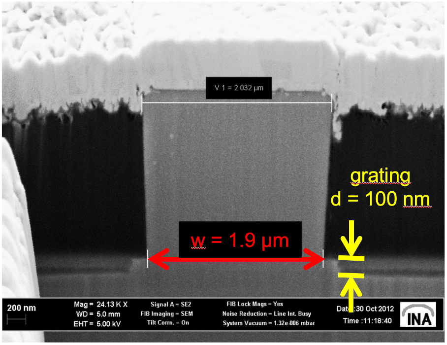 Image: Technische Physik
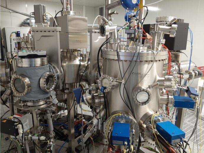 Image: Technische Physik
- In which other areas can (your) quantum dots be used?
Prof. Dr. J.-P. Reithmaier: Here at the department, we also deal with secure data transmission based on quantum effects. When I transmit data via optical fiber, the signals are modulated, sometimes with more intensity, sometimes with less. However, while the data is being transmitted, I can theoretically detect it and read out the data. But if it's an encryption code, for example, then you shouldn't make it public and it's difficult to transmit it over a fiber. With certain quantum communication methods, we can transmit data via individual photons (light quanta) and at the same time ensure that no one else can intercept the data. If data is transmitted via individual photons, it immediately becomes apparent that a photon is missing and the transmission can be repeated. We use quantum dots to generate these individual photons. If I bring charge carriers together again here, then a photon, i.e. a quantum of light, is emitted in my quantum dot. The properties of these quantum dots ensure that only one photon is produced. This area is under development. Then there is the field of quantum computing or quantum sensor technology, where these nano-structures of quantum dots are very important. Quantum computing is about data processing. In quantum sensor technology, it is possible to use quantum dots to improve the sensor technology of certain devices and techniques, such as microscopes and measurements at the nano level.
- Dr.-Ing Hartung, your aim is to integrate functions into plastics. What is the advantage of this?
Dr.-Ing. M. Hartung: When it comes to plastics, many people think of packaging and everyday objects such as cell phones and kitchen utensils. Here they fulfill the purpose of shaping and geometry. However, if you add electrical, magnetic, heat or light-conducting particles such as quantum dots to a plastic, these functions are integrated into the plastic. Plastic components can therefore conduct electrical signals, dissipate heat as battery housings or, when it comes to quantum dots, absorb and transmit light. In addition to the addition of particles, a function can be integrated into a plastic via a layer system. This makes it possible, for example, to darken translucent plastics at the touch of a button or to build simple sensors or actuators using so-called electroactive polymers. In all applications, processing plays a decisive role in whether the function is retained in the plastic. This is what makes the integration of functions so interesting for us engineers, because we want to use our research to facilitate the transfer of technologies from laboratory scale to industry.
- So you can also integrate quantum dots into plastic? What is special about quantum dots for you as engineers?
Dr.-Ing. M. Hartung: Yes, exactly. We use quantum dots similar to those developed by the Nobel Prize winners in chemistry. Due to their small size in the nanometer range, they have special properties in terms of their interaction with light. As already described by Prof. Reithmaier, they can transform into other wavelengths depending on their size when exposed to light, a phenomenon known as "quantum shift". This effect is also advantageous in photovoltaic technology. Mixed into transparent plastics, these unique properties of quantum dots can be used for electricity-producing windows.
- Producing electricity with a window - that sounds exciting! Mr. Koch, you have used quantum dots to develop a smart and efficient building-integrated photovoltaic system. How did you go about it and how does the technology work?
M.Sc. M. Koch: We have integrated quantum dots into a transparent plastic film that is applied to the glass pane of a window. These quantum dots, which are between 8 and 12 nanometers in size, are first inserted into a plastic wax as a carrier material and then processed into film. The sun's rays are partially absorbed on the film. The radiation is then re-emitted with a red shift and partially trapped in the glass. The trapped radiation is converted into electrical energy at the edge of the window by attached photovoltaics and can be used there. The principle behind this is LSC technology.
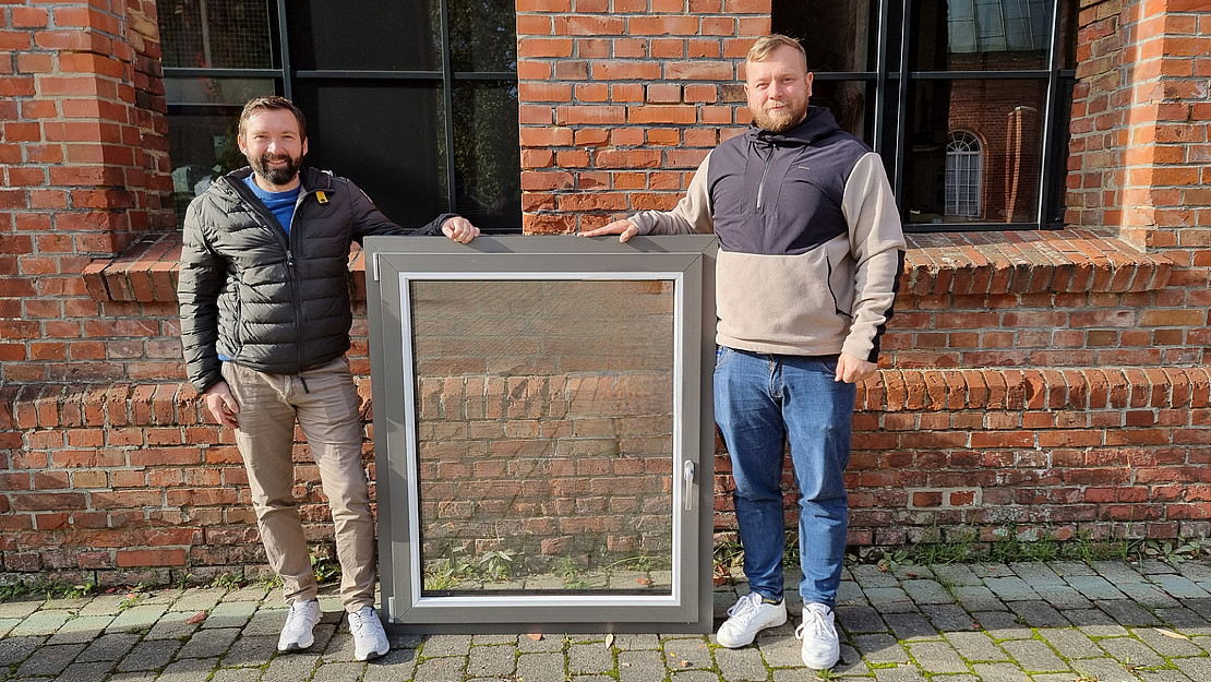 Image: ifw
- What is special about this technology and how far along are you in its development?
M.Sc. Matthias Koch: The aim is to use window areas to generate energy. By absorbing sunlight and emitting it in the near-infrared and infrared range, the quantum dots ensure that electromagnetic radiation can be "captured" in the window glass light guide. There, the radiation is brought to the edge of the window via total internal reflection, where photovoltaics are installed. There, the energy is then converted into electrical energy and is available for use. With this innovative technology, it is now possible to integrate energy generation in buildings in places that were previously inaccessible.
Prof. Dr. J.-P. Reithmaier: It is also possible to use highly efficient detectors at the edge of the window because you don't have to use them over a large area. A few 10-100 square centimetres may be enough here, whereas solar cells on the roof can take up 100 square meters to generate the same amount of energy. You can then afford to pay a factor of 100 more for the solar cells that are installed. This is definitely a good example of developing new intelligent materials that make it possible to combine materials with different functions.
- When will the technology be able to be used on buildings on a large scale?
M.Sc. M. Koch: A demonstrator window from Walter Fenster + Türen Kassel, which was developed in collaboration with us, is soon to be installed on the Vonovia company building in Kassel Waldau. Unfortunately, however, the film is not yet being used, as it has not yet been produced in the required size due to the very small quantities of quantum dots available. We hope to find partners in the future who can produce sufficient quantities so that this technology can be used.
- This brings me to my last question. The integration of new functions into different materials can lead to an increase in efficiency and thus help to conserve natural resources. This is one of the aims of the BiTWerk - Biological Transformation of Technical Materials research cluster, to which more than 20 professors from the University of Kassel belong. You are also part of the cluster with your specialist areas. How do you classify your research there?
Dr.-Ing. M. Hartung: The aim of BiTWerk is to consider components and their resulting material properties as an inseparable unit, starting with the production processes, through use to recycling, in order to establish a fully biologized process chain. To this end, various Faculties at the University of Kassel are working together on an interdisciplinary basis. Plastics technology is a central component here, as the integration of as many functions as possible into plastics by means of molecular nano- and micro-components avoids the production of many individual components with individual functions and thus reduces the ecological footprint.
Prof. Dr. J.-P. Reithmaier: In line with the BiTWerk research cluster, we at our department also always aim to use our research to help minimize the impact of manufacturing techniques and materials on the environment and to develop new functional materials for applications. To this end, a DFG project was recently approved to develop the fundamentals of novel nanostructured optoelectronic materials that do not occur in nature. In parallel, an EU-wide joint project with partners from research and industry has been applied for to investigate the application potential, again addressing the optical properties of quantum dots. The semiconductor material silicon is at the center of the research. The production of optically active semiconductors using materials such as arsenic, gallium, indium or aluminum is complex, expensive and harmful to the environment. Silicon, however, can be easily extracted from many different raw materials, e.g. silicates, which are the main component of the earth's crust. Furthermore, the waste from silicon does not pollute nature. The semiconductor material has only one disadvantage: it cannot be used to produce light itself. Therefore, silicon cannot be used for the production of light-emitting diodes or lasers. We are now trying to modify the properties of the silicon material itself so that it is just as suitable for the production of optically active semiconductors as the existing compound semiconductors (GaAs, InP, etc.). This would save at least four orders of magnitude in environmentally harmful materials and contribute to sustainability on earth.
Further information:
INA - Institute for Nanostructure Technology and Analytics
https://www.uni-kassel.de/forschung/ina/institut-fuer-nanostrukturtechnologie-und-analytik-ina/
CINSaT - Center for Interdisciplinary Nanostructure Science and Technology
https://www.uni-kassel.de/forschung/cinsat/startseite
Application Center UNIfipp