Highlights concerning 3D Nanostructurization
Nanospectrometer
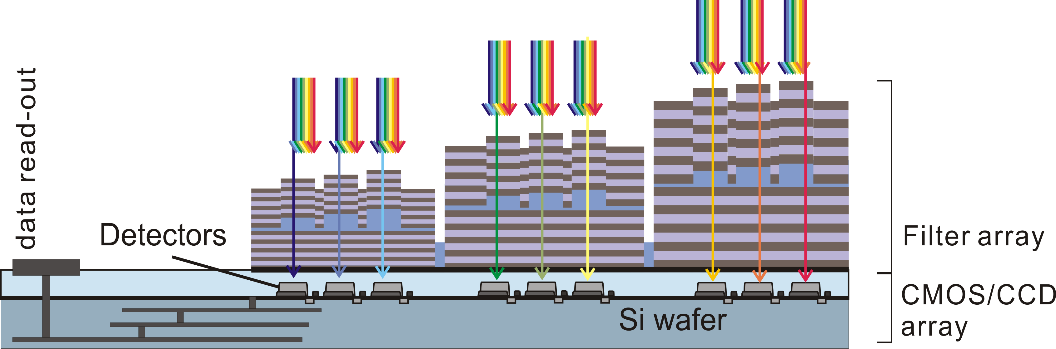
The ubiquitous usage of optical metrology in daily life is crucially dependent on cost, size and mobility. To combine these demands is very challenging and is targeted in our novel miniaturized spectrometer. A filter array combined with a sensor array is a spectrometer. Since Nanoimprint is used for the fabrication of the filter array (to improve spatial resolution and to decrease fabrication cost) we call it ‘Nanospectrometer’. Our final goal is that the Nanospectrometer will be able to detect for example biomarkers in the skin, health status, quality of food, and concentrations of harmful trace gases in traffic and industrial production. A further advantage of optical sensorics is, that they do not need to get in direct contact to the object of interest. Conventional grating spectrometers suffer from decreasing resolution, the higher the degree of miniaturization (if the grating size is shrinking, the number of illuminated grating lines is decreasing). Note that the grating period has to be kept constant during miniaturization.
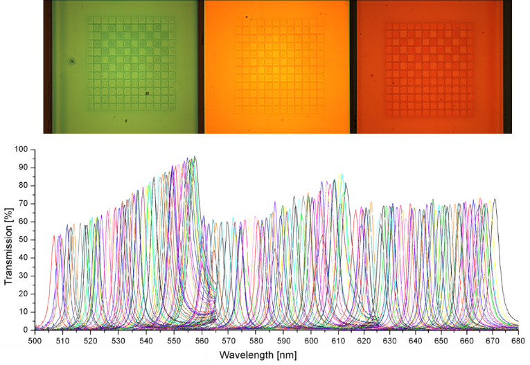
The Nanospectrometer consists of many individual Fabry-Pérot filters combined in a filter array, which is directly placed on commercial CCD or CMOS chips. The latter imaging chips are well-known from applications in e.g. digital cameras. Each individual filter is addressing a low number of pixels (e.g. 9) of the CCD or CMOS chip. This way, this pixel group detects an individual narrow band (1-3nm linewidth of the filter line, revealing very high spectral resolution). Nanoimprint technology allows to fabricate the 3D structured cavity layer of thousands of Filter arrays in a single printing step and with a sub-nm resolution in the vertical direction. Worldwide our group has achieved the highest resolution in the third dimension in Nanoimprint. A drawback is the limited spectral stopband-width of the Bragg mirrors in the range of 100nm. However, applications require a larger total spectral range which requires the combination several stopbands and implies different total thicknesses of the corresponding Bragg mirrors (this implies to print over multiple steps instead on a flat surface (Fig.1). The different thicknesses of the three Bragg mirror stacks are revealing a different color in Fig.2 top, showing a noticeable step where the color is changing. Another highlight is that we succeeded to print over these steps. Each of the three stopband includes 64 different cavity heights, which gives a total number of 3 x 64 = 192 different cavity heights and 192 pixels. Note, that even the best digital camera is based only on 3 spectrally different pixels (RGB technology). Fig. 2 bottom demonstrates, that we have the complete 192 filter lines - not even one is missing, another highlight.
Recording of spectra is achieved by reflecting all light coming from the substance to the filter except of a single well-defined wavelength which is transmitted by the filter and can be detected by the sensor. In the EU project “Bread Guard”, we built a fully functionable demonstrator for the visible range and tested it to monitor the baking process in a commercial modern deck oven. In addition, we demonstrated the Nanospectrometer principle also in the near infrared. In future, we wish to integrate our technology also in smart mobile phones: Changes in the spectra would reveal information about health status, food quality, allergic substances and air quality.
BMBF project “Nanoscale”
Smart Window “Nanoscale” for personal lighting, energy saving and health
Today, limiting global warming, carbon dioxide emission reduction, sustainable energy production, and efficient energy saving are worldwide key challenges. The sustainable design of ‘green buildings’ has become increasingly important in the last few decades and the use of natural light has become an important strategy to improve energy efficiency by minimizing lighting, heating, and cooling loads as well as to stabilize bio rhythm and to improve human health. In general, the implementation of efficient daylighting strategies can considerably reduce electricity consumption in buildings, since artificial light, cooling, and heating constitute by far the largest part of the total energy consumption in nonresidential buildings.
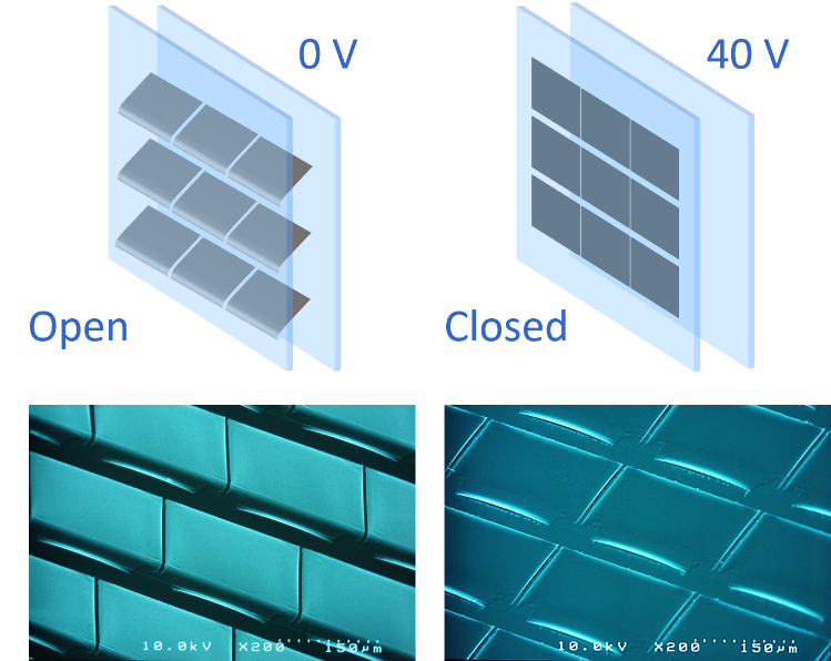
Our MEMS concept is using millions of micromirrors inside insulation glazings to guide and control light by electrostatic mirror actuation. This enables energy saving, tailored personalized lighting, security, and smart personalized environments in buildings. The window transmission is controlled continuously, showing the eye a variable-tone pane. The amount, direction, and degree of steering of the guided light are tailored to winter, summer, and variable daytime requirements, protecting rooms and persons inside from sun- light while providing tailored natural daylight illumination.
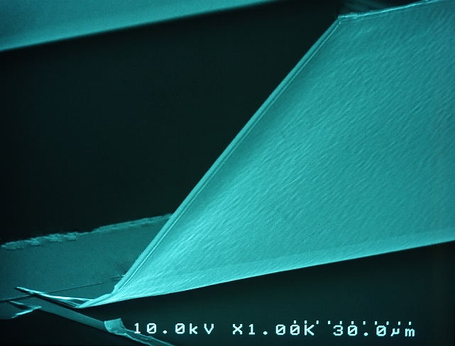
Millions of micromirrors, arranged side by side, have been implemented between two or more panes of insulation windows. Depending on the requirements, the micromirrors are tilted at different angles via electrostatic actuation. Such micromirrors have a size of less than 0.1 mm² (although they vary a lot, typical dimensions are 150 × 400 µm2), which means more than 12,000,000 mirrors/m². The layer design of the mirrors includes multiple layers nanoscale in thicknesses (transparent conducting oxides, insulating oxides and different metals). Owing to the small size of the micromirrors, the naked eye cannot identify single mirror elements from distances >20 cm.
Micromirror arrays have been designed, fabricated, and characterized. Experimental results on electrostatic actuation voltages, extrapolated lifetime, power consumption, and heat impact regulation have been investigated in 2 EU projects “MEM4WIN” and “NEXT Buildings” as well in the BMBF project “Nanoscale”. The acronym stands for Nano Sensors and Actuators for smart personal Environments. The measured high resonance frequencies of 3kHz, long lifetimes in long-term actuation tests, low power consumption of as low as 0.2 mW/m2 and the actuation voltages of as low as 12 V show the potential, but a lot of work still remains to be done.

Functional 3D Nanoparticles:
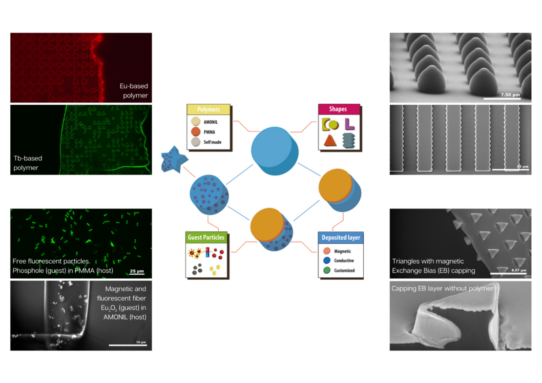
“Multifunctional Anisotropically Shaped Hybrid-Particles" (MASH) is a joint research project coordinated by Hartmut Hillmer in collaboration with the CINSaT members, Arno Ehresmann and Rudolf Pietschnig. MASH combines several defined technological, physical and chemical tasks. The 3 CINSaT groups from different disciplines combine the expertise in their fields to target interdisciplinary fundamental research, 3D micro- and nano-structurization, characterization and applications of 3D micro- and nanoparticles.
Polymer micro- and nanoparticles have a wide variety of applications in liquid environments, such as molecular transporters, microsensors, contrast agents in medical diagnostics and customized filter systems for our environment. For these types of applications and many others, the particles are chemically functionalized by reactive molecular groups on their surface, which serve as binding sites for analytes. In general, spherically shaped particles are more widely encountered than geometrically more complex shapes, due to the fact that most fabrication techniques are bottom-up approaches mostly driven by thermodynamic interactions, where the most energetically favorable outcome is a sphere. From a modeling point of view, the system also becomes increasingly more complicated the more parameters/asymmetries are added to it. However, it has been shown that the spherical shape of the particles brings about numerous limitations when used in a confined hydrodynamic environment. Here, the anisotropic non-spherical particles reveal advantages in terms of wall-interactions and adhesion, amongst others, which give access to more degrees of freedom of the particle movement. Besides the variation of size and shape the functionalization of the polymer particles plays a key role in the project MASH. By adding capping layers via metal deposition on the surface magnetic and conductive properties or binding sides for molecules are added to the particle. For further functionalization nanoparticles are implemented in a guest-like manner into the polymer-host particle. By combining the surface and guest-like functionalization multifunctional particles with specific properties (e.g. magnetic, fluorescent, conductive) are fabricated. These multifunctional particles can be used for different applications e.g. transport, magneto-fluorescent markers or carriers for biomolecules, among others.
(Kopie 12)
Contact
Prof. Dr. rer. nat. habil. Hartmut Hillmer
full member

- Telephone
- +49 561 804-4485
- hillmer[at]ina.uni-kassel[dot]de
- Location
- Universität Kassel
Fachbereich 16 - Elektrotechnik & Informatik
Institut für Nanostrukturtechnologie und Analytik
Heinrich-Plett-Straße 40
34132 Kassel
- Room
- 2113