Research
The research group Nanophotonics investigates and develops structures, devices and methods in the fields of optoelectronics, nanotechnology, thin-film technology and related technological methods. The results of our research activities are applicable to sensors, light emitters, data transmission and material processing.
Our general approach is based on periodic arrangements of different materials as well as the tailored disturbance of their order by either local defects or distributed variations. Optical thin-films structures with 1D periodicity are investigated regarding their application in new filters and laser devices (VCSEL). Periodic structures in 2D or 3D are considered in our research of photonic crystals, fano resonances and plasmonic effects. These structures can be implemented as devices themselves or integrated with MEMS elements or on the tip of optical fibers. A wide range of materials, like semiconductors, dielectrics, metals, organic compound, for example polymers, as well as some special materials are available for use. Thus our structure can be optimized with different applications, spectral ranges or certain design goals in mind.
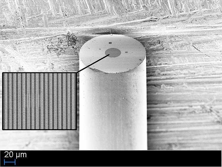
High-resolution nanoimprint technology, the use of focused ion beam (FIB) and plasma enhanced processes are used for the generation of nanostructures at INA. The design of devices and structures, is based on numerical simulations of optical, electrical, mechanical and quantum mechanical properties. The analytical equipment at the institute is employed for precise characterization of nanostructures, optoelectronic devices and technological processes.