Home
INA, Technische Physik
![[Translate to English:] Figures](/forschung/files/INA/Technische-Physik/Fotos/TP_figure_band_800.png)
Welcome
The department "Technische Physik" is engaged in the fabrication and characterization of nanostructured materials and their applications in novel devices. A major focus lies on semiconductor nanostructures and optoelectronic as well as nano-photonic devices, which are dedicated for classical optical communication as well as for quantum information processing or communication.
For the fabrication of nanostructured materials the "top-down" approach (i.e., macroscopic materials are downscaled ot nanometer dimensions by high-resolution lithography and etching techniques), as well as the "bottom-up" approach are used (i.e., nanostructures develop themselves via self-organization effects from atomic or molecular components). In this sense new fabrication methods are developed and their quantum mechanical effects as well as their impact on macroscopic materials and device properties are studied.
An example are semiconductor quantum dots, whose optical properties are investigated in dependence of geomterical features. Semiconductor quantum dots of high densitiy and tailored geometrical sizes are used in semiconductor lasers to optimize specific material properties for specific applications, e.g., spectral optical gain by so-called "gain-engineering". With those nanoscaled materials, one can obtain device properties, which are impossible to reach with conventional techniques.
In the area of quantum information processing different material systems are used. On one hand also semiconductor quantum dot structures are applied, however, which are very often integrated in micro or nano cavities enhancing drastically the light-matter interaction. With those techniques also the interaction and control of single particles is possible, such as photons and charge carriers. On the other hand, color centers, like nitrogen-vacancy centers in crystalline diamond, are used due to their excellent long-time stability of quantum states in particular by considering solid state systems
The department is also targeted very interdisciplinary and works together with groups from engineering, biology and chemistry on topics, which are originated from the different disciplines. For example, the development of new sensor systems on the basis of nanostructured semiconductor materials, the immobilization of single molecules on functionalized diamond surfaces and the realization of electrical/biological interfaces with neurons.
An overview on topics are given in the Overview Poster.
Research Groups
The department is divided in four research groups. Each of them is focussed on a specific research topic.
Prominent Highlights
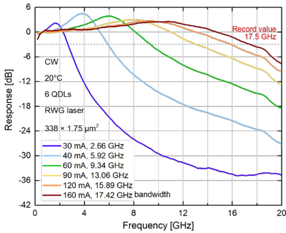
Temperature stable high-speed 1.5 µm quantum dot lasers
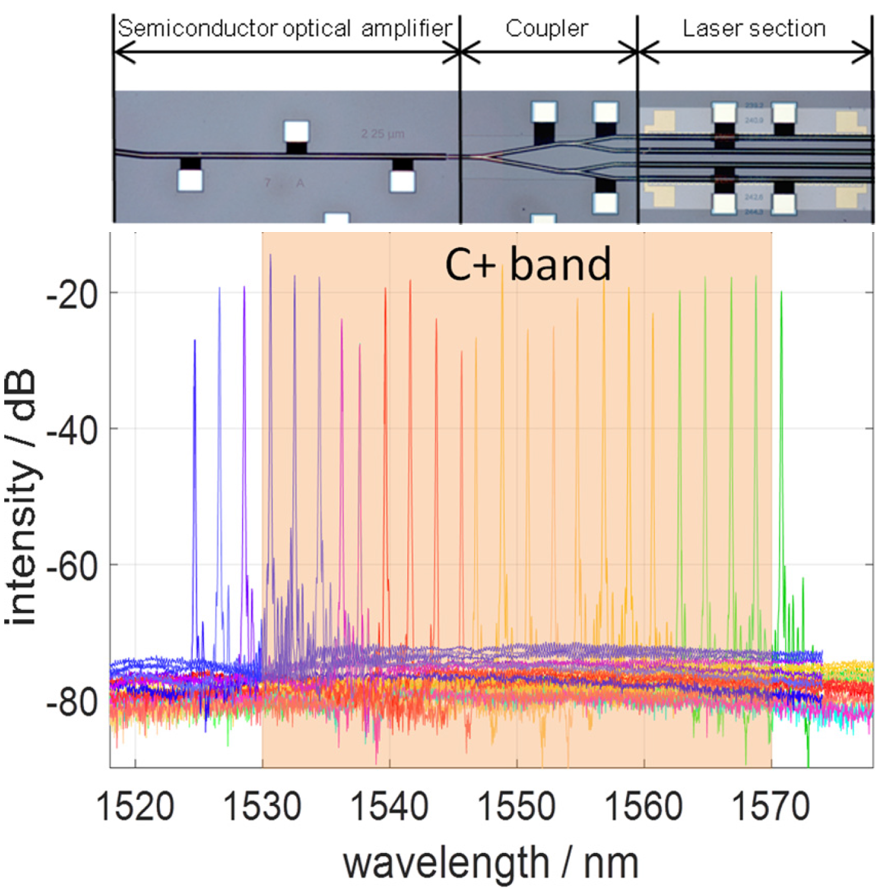
Ultra-narrow widely tunable quantum dot laser chip
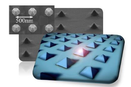
Deterministic Arrays of Epitaxially Grown Diamond Nanopyramids with Embedded Silicon‐Vacancy Centers
For more information see
J. Tzach et al., Advanced Optical Materials 7, 1800715 (2019).
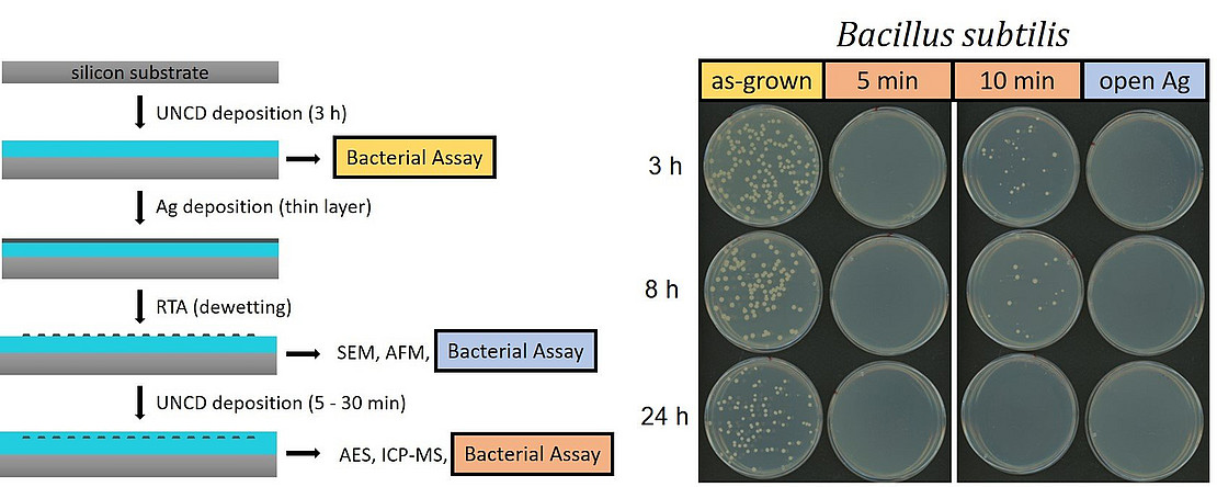
Antimicrobial propensity of ultrananocrystalline diamond films with embedded silver nanodroplets
For more information see
D. Merker et al., Diamond and Related Materials 93, 168 (2019)
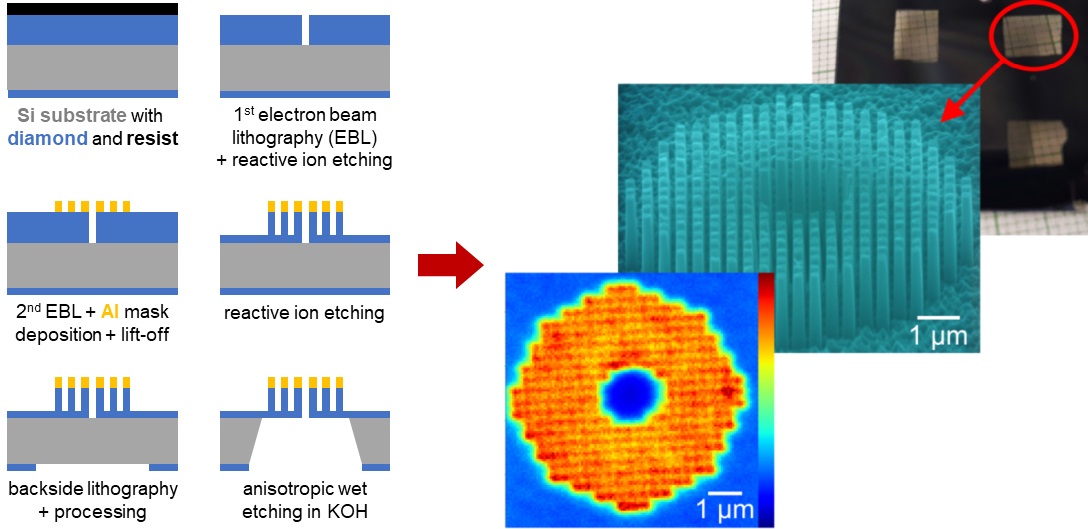
Fabrication of Nanopillars on Nanocrystalline Diamond Membranes for the Incorporation of Color Centers