Nano Materials
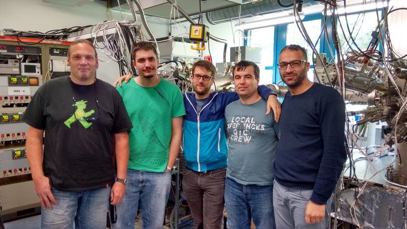
Group Members
| Group Leaders | Vitalii Sichkovskyi, Johann Peter Reithmaier |
| PhD Students | Balasubramanian Ramasubramanian, Vinayakrishna Joshi |
| Technicians Master Students | Dirk Albert |
Objectives
One- and zero-dimensional semiconductor structures attract significant research interest due to their unique electronic and optical properties, based on quantum confinement of the electron and hole motion. One of the major goals of our group is the development and optimization of zero-dimensional structures, known as quantum dots (QDs), which should contribute to the development of new optoelectronic devices with significantly improved performance.
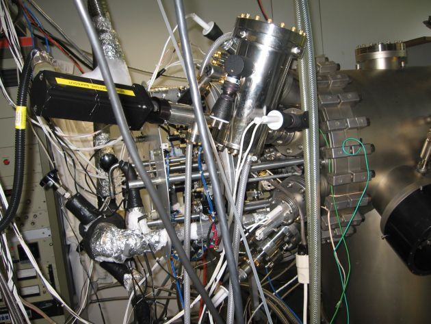
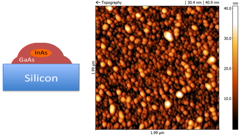
The mostly used method for the growth of quantum dot structures is based on self-assembled Stranski-Krastanov growth mode by molecular beam epitaxy (MBE), which can be combined with pre-patterning of the substrate by electron beam lithography, allowing control of the density and dimensions of the structures.
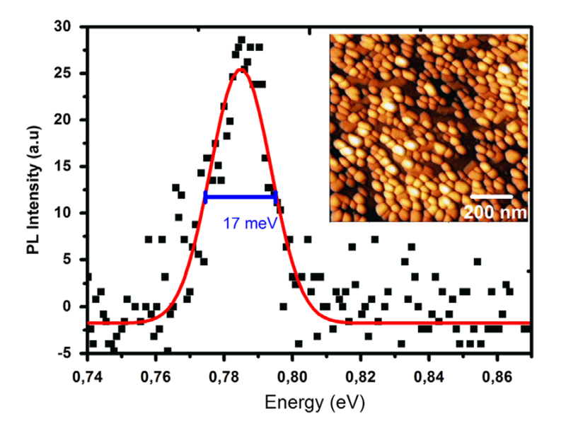
Our current research activities are focused on the investigation of the influence of the MBE process parameters on the formation and growth of quantum dot structures, based on GaAs, InP, and Si substrates by Varian Gen II MBE system. The density and morphology of the QDs are assessed using atomic force microscopy. Their optical properties are characterized ex-situ by low-temperature photoluminescence (PL) spectroscopy.
Projects
Literature
Publications
- S. Banyoudeh, J.P. Reithmaier, "High-density 1.55 µm InAs/InP(100) based quantum dots with reduced size inhomogeneity", J. Cryst. Growth 425, 299 (2015) (pdf-File)
- A. Maryński, G. Sęk, A. Musiał, J. Andrzejewski, J. Misiewicz, C. Gilfert, J.P. Reithmaier, A. Capua, O. Karni, D. Gready, G. Eisenstein, G. Atiya, W. D. Kaplan, S. Kölling, "Electronic structure, morphology and emission polarization of enhanced symmetry InAs quantum-dot-like structures grown on InP substrates by molecular beam epitaxy", J. Appl. Phys. 114, 094330 (2013) (pdf-Datei)
- V.I. Sichkovskyi, M. Waniszek, J.P. Reithmaier, "High-gain wavelength-stabilized 1.55 µm InAs/InP(100) based lasers with reduced number of quantum dot active layers", Appl. Phys. Lett.102, 221117 (2013) (pdf-Datei)
- A. Capua, O. Karni, G. Eisenstein, V. Sichkovskyi, V. Ivanov and J.P. Reithmaier, "Coherent control in a semiconductor optical amplifier operating at room temperature", Nature Communications 5, 5025 (2014) (pdf-Datei)
- V. Sichkovskyi, V. Ivanov, J.P. Reithmaier "High Modal Gain 1.5 µm InP based Quantum Dot Lasers: Dependence of Static Properties on the Active Layer Design", Photonics West Conf., San Francisco, USA (February 2013)
Overview talks
Picture gallery
![Cross-sectional high-angle annular dark-field scanning transmission electron microscopy (HAADF-STEM) micrograph of the InAs/InAlGaAs/InP QDs structure viewed in the [110] direction (perpendicular to the QDs elongation direction).](/forschung/files/INA/Technische-Physik/Forschung/Nano_Materials/Fotos/InAs-on-InP-TEM-small.png)