Nano Fabrication & Devices
Group Members
| Group Leader | Johann Peter Reithmaier |
| PhD Students | Alireza Abdollahinia, Annette Becker |
| Technicians: | Anna Rippien, Florian Schnabel, Kerstin Fuchs |
Objectives
The "Nano Fabrication & Devices" group deals with the development of novel fabrication processes on the basis of high-resolution lithography (e.g., electron beam lithography) and dry etching techniques for the realization of semiconductor nano structures. Those techniques are used for the fabrication of optoelectronic devices, such as semiconductor lasers, amplifiers, optical switches, optoelectronic integrated circuits (OEICs), and more.
In addition, the group deals with the characterization of fabricated structures and devices. Special tools were constructed for the characterization of novel devices (e.g., fiber based linewidth measurement set-up, high-frequency set-up for small signal modulation, set-up for chirp measurement, and more). Also standard measurement tools are used for the basic characterization of lasers in pulsed and continous wave mode.
Projects
- EU-Project "SEQUOIA"
- BMBF-Project "Monolop/SASER"
Literature
Publications
- S. Combrié, G. Lehoucq, A. Junay, S. Malaguti, G. Bellanca, S. Trillo, L. Ménager, J.P. Reithmaier, and A. de Rossi, "All-optical signal processing at 10 GHz using a Photonic Crystal Molecule", Appl. Phys. Lett. 103, 193510 (2013) (pdf-Datei)
- D. Gready. G. Eisenstein, V. Ivanov, C. Gilfert, F. Schnabel, A. Rippien, J.P. Reithmaier, "High-speed 1.55 µm InAs/InGaAlAs/InP quantum dot lasers", IEEE Phot. Technol. Lett. 26 (1), pp. 11-13 (2014) (pdf-Datei)
- A. Becker, M. Bjelica, V. Sichkovskyi, A. Rippien, F. Schnabel, P. Baum, B. Witzigmann, J.P. Reithmaier, "InP-based narrow-linewidth widely tunable QD-DFB lasers", VDE-ITG meeting, Leipzig, Germany (May 2015) (pdf-File)
- S. Banyoudeh, A. Abdollahinia, V. Sichkovskyi, J.P. Reithmaier, "1.5 µm quantum dot laser material with high temperature stability of threshold current density and external differential efficiency", Photonics West Conf., San Francisco, CA, USA (February, 2016). Proc. SPIE 9767, Novel In-Plane Semiconductor Lasers XV, 97670I (March 7, 2016) (pptx-File, 2 MB) (pdf-File of proceed. paper)
- S. Banyoudeh, A. Abdollahinia, O. Eyal, F. Schnabel, V. Sichkovskyi, G. Eisenstein, J.P. Reithmaier, "High-speed directly modulated 1.5 µm quantum dot lasers", Photonics West Conf., San Francisco, CA, USA (February, 2016). Proc. SPIE 9767, Novel In-Plane Semiconductor Lasers XV, 97670L (March 7, 2016) (pptx-File, 9 MB) (pdf-File of proceed. paper)
- A. Becker, V. Sichkovskyi, M. Bjelica, O. Eyal, P. Baum, A. Rippien, F. Schnabel, B. Witzigmann, G. Eisenstein and J.P. Reithmaier, "Narrow-linewidth 1.5 μm quantum dot distributed feedback lasers", Photonics West Conf., San Francisco, CA, USA (February, 2016). Proc. SPIE 9767, Novel In-Plane Semiconductor Lasers XV, 97670Q (March 7, 2016) (pptx-File, 7 MB) (pdf-File of proceed. paper)
Overview Talks
- J. P. Reithmaier, G. Eisenstein, A. DeRossi, S. Combrié, "Power Saving in Communication Applications by Nano-Structured Optoelectronic Components", Technion / TU Berlin Green Photonic Symposium, Berlin (invited, March 2015) (pptx-File, 25 MB)
- J.P. Reithmaier, "Nanostructured Materials for Optoelectronic Devices: Current Developments and Future Challenges", Int. Symp. on Advances in "Quantum Materials, Quantum Physics and Nanophotonics", Würzburg, Germany (invited, April 2015) (pptx-File, 93 MB)
- J.P. Reithmaier, S. Banyoudeh, A. Abdollahinia, V. Sichkovskyi, A. Becker, A. Rippien, F. Schnabel, B. Bjelica, B. Witzigmann, O. Eyal, G. Eisenstein, "The impact of low-dimensional gain material on emission linewidth and modulation speed in semiconductor lasers", Conf. on Physics of Quantum Electronics (PQE), Snowbird, Utah, USA (invited talk, January 2016) (pptx-File, 8 MB)
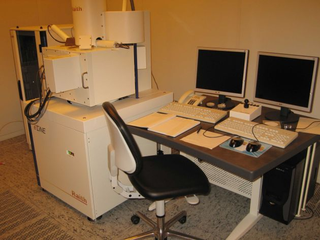
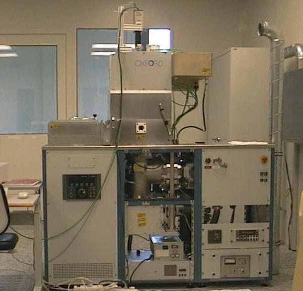
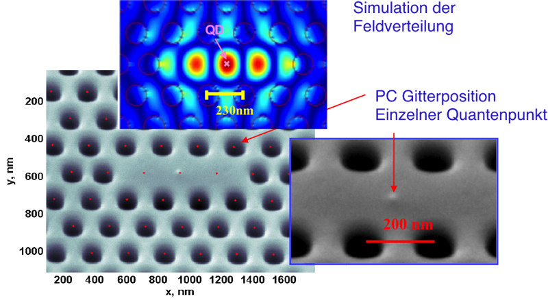
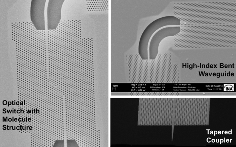
Picture gallery