Equipment
Lithography
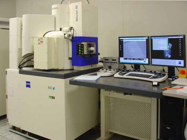
Zeiss NVision 40 High End Cross Beam
- Electron column: high resolution (1,3nm) field emission
- Ion column: high resolution (4nm), suitable for deposition and etching
- Fabrication of TEM-Samples and analysis in transmission
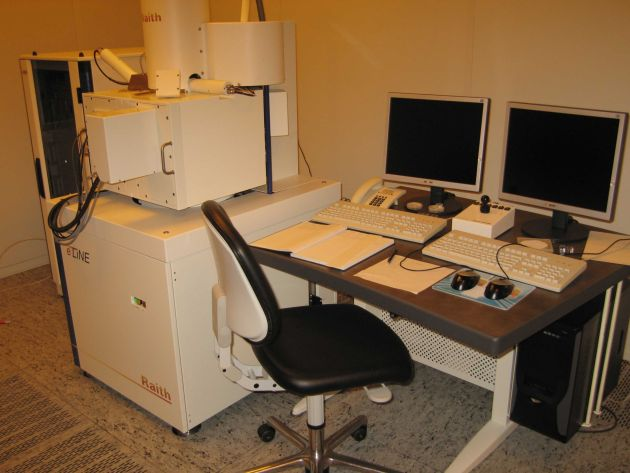
Raith eLine Electron Beam Lithography
- High resolution (20nm and below)
- 100 x 100 mm laser interferometer table
- Positioning accuracy 2nm in x- and y-direction
- 1,6nm beam diameter
- Stitching free exposure by FBMS (Fixed Beam Moving Stage) & MBMS (Modulated Beam Moving Stage)
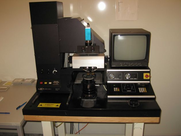
Karl Süss MA4 Maskaligner
- up to 4"-substrates, up to7"-masks
- Resolution: standard 800nm, optional up to 300nm
EVG Al-4 Maskaligner
- up to 4"-substrates, up to 5"-masks
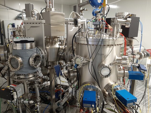
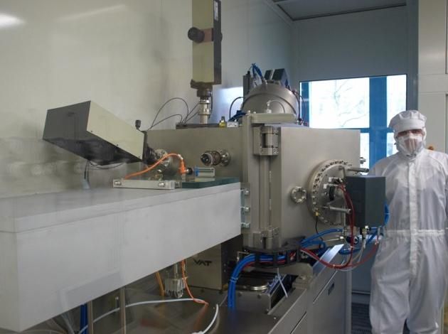
Epitaxy Systems
8'' Dual chamber molecular beam epitaxy system (Dr. Eberl MBE-Komponenten GmbH)
- Coupled reactors for III-V semiconductor & SiGe layers
- Semiautomatic sample transfer via central chamber, hydrogen cracker (H)
- Very god layer thickness homogeneity, temperature homogeneity and doping homogeneity
- Ultra high vacuum (10E-10 - 10E-11 mbar)
- In-situ control using RHEED
- Material Reactor C: Ga, In Al, As2, P2, Si, Be
- Material Reactor D: Si, Ge, B, P
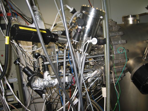
Varian Gen II Modula MBE
- Coupled systems for GaAs and InP growth
- Sub-nm layerthickness control
- In-situ-control by RHEED / Ultra High Vacuum ( 10E-8 - 10E-10 mbar )
- Materials : Ga, In, Al, As2, Si, Be
- Reactor A: Silicon E-Beam-Evaporator, Hydrogen-Cracker (H)
- Reactor B: Phosphorus-Cracker
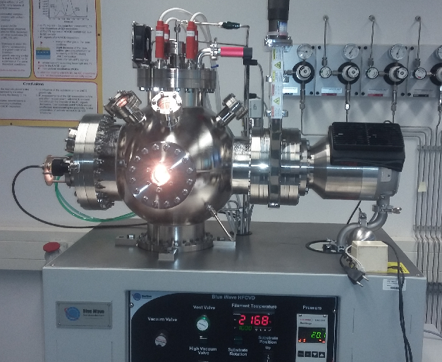
Bluwave HFCVD
Hot Filament Chemical Vapor Deposition
- Process gases: Methane (CH4), Hydrogen (H2), Nitrogen (N2)
- Materials: Poly- and nanocrystalline diamond films (PCD, NCD)
- Deposition of diamond films as well as overgrowth of diamondsubstrates
AsTex MWCVD
MicroWave Plasma Chemical Vapour Deposition
- Process gases: methane(CH4), hydrogen(H2), nitrogen(N2), argon(Ar), oxygen(O2)
- Materials: Poly- and nanocrystalline diamond films (PCD and NCD)
Deposition
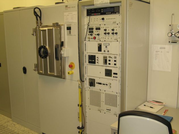
Roth ß Rau Ionsys 1000 IBD
Ion Beam Deposition
- Class 1 cleanroom section
- Multilayer systems (DBR,VCSEL,etc.)
- In-situ process control
- Material: metals(e.g. Al,Zr,Cr), oxides(e.g.ITO,TiO,SiO2), nitrides (e.g. Si2N3)
- Process gases: Argon(Ar), Xenon(Xe), Oxigen(O2), Nitrogen (N2)
Pfeiffer PLS 500 Evaporation System
- Thermal or electron beam
- Materials: Titan(Ti), Nickel(Ni), Chrom(Cr), Platin(Pt), Aluminium(Al)
Balzers BAK 600 Evaporation System
- Thermal or electron beam
- Processgas: Argon (Ar)
- Material: Nickel (ni), Titan (Ti), Platin (Pt), Gold (Au), Germanium (Ge), Chrom (Cr)
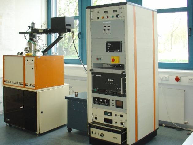
Oxford Plasmalab 80 PECVD
Plasma Enhanced Chemical Vapour Deposition
- Process gases: Silan (SiH4), Hydrogene (H2), Ammonia (NH3), Nitrous oxide (N20)
- Material: Silicon Nitride (SiN), Silicon Oxide (SiO), Silicon (Si)
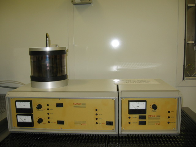
Emitech K550 Sputter Coater
- Process gases: Argon (Ar)
- Material: Platinum (Pt)
Dry Etching Systems
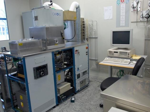
2 Oxford Plasmalab 100 ICP-RIE
Inductive Coupled Plasma - Reactive Ion Etching
- ICP 1: for deep etching of silicon with flourine-donators (Bosch-Prozess)
- ICP 2: for etching of semiconductor materials (e.g. GaAs) with chlorine-donators
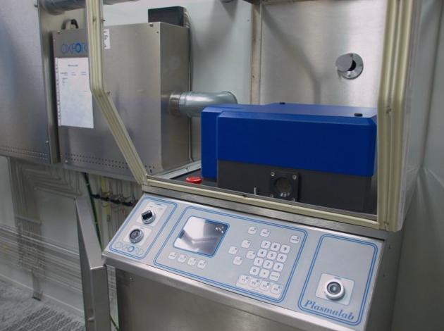
Oxford Plasmalab 80 Plus RIE
Reactive Ion Etching
Parallel Plate Reactor
- Process gases: Hydrogen (H2), Methan(CH4)
- Material: Indium(In), Phosphorus(P), Gallium(Ga), Arsenic(As) compound semiconductors
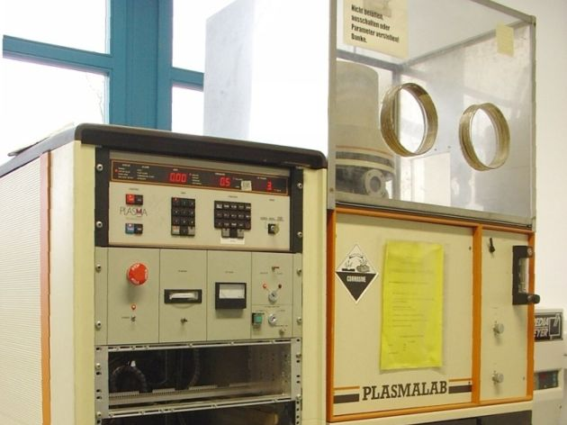
Plasmalab RIE
Reactive Ion Etching
- Etching of BCB, SiO2, SiN, Si
- Process Gases: CHF3, Ar, SF6, O2
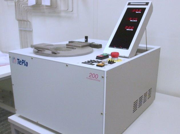
TePla 200-G Oxygen Asher
- Etching of photo resist and organic residues
- Process gas: Oxygen(O2)
Other Devices
Xerion RTA
Rapid Thermal Annealing
- Process gas: Argon (Ar)
- Temperatures up to 400°C
RTA
Rapid Thermal Annealing
- Process gas: Argon (Ar), Nitrogen (N2)
- Temperaturecontrol by Thermoelement or Pyrometer
- Temperatures up to 1300°C
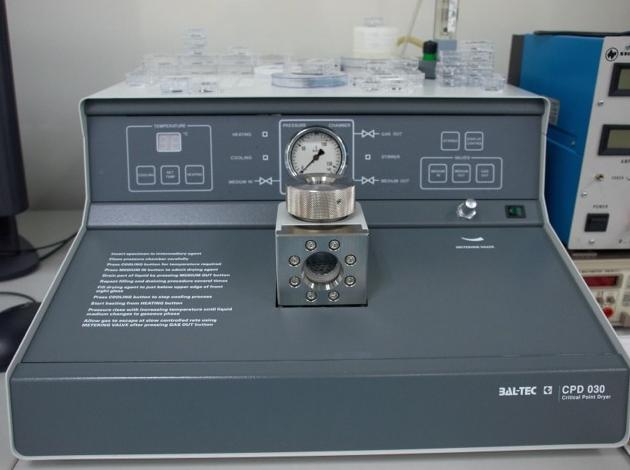
Bal-Tec CPD 030 Critical Point Dryer
Process gas: Carbon Dioxide(CO2)
Analytics
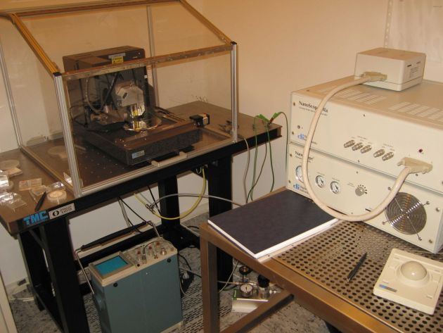
AFM Nanoscope Dimension 3100
- Atomic Force Microscopy with Contact- and Non-Contact-Modus
- Wafer up to 6" diameter
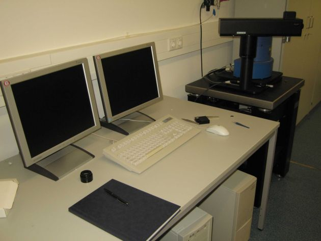
AFM CP-II
- Atomic Force Microscopy with Contact- and Non-Contact-Modus
- Scanning Tunnelling Microscopy
- Nanolithography
DualScopeTM 95 SPM System
- The DualScopeTM 95 SPM scanner provides the facilities for all common and advanced SPM modes.
- Integrated electronics in the scan head guarantees lowest noise values in electrical SPM modes.
- Supported Modes: Contact mode (DC), intermittent mode (AC), non-contact mode, frequency modulation mode, lateral force mode, force spectroscopy, EFM, MFM, STM
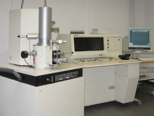
2 Scanning Electron Microscopes / Hitachi s-4000 and s-4100
- Resolution: 1,5nm at 30kV, WD 5mm
- Magnification: 20x to 300000x
- Accelerating voltage: 0,5 to 30kV
- s-4000: Active image acquisition/processing system DISS 5
- s-4100: Energy dispersive spectrometer EDAX DX-4, Backscattered electron detector
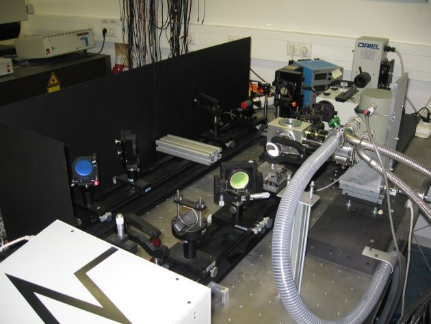
Spectroscopy Set-up
Absorption- and Photoluminescence-Spectroscopy
- Temperature control down to 10K
- Sub-nm spectral resolution
- Si-photodiode and InGaAs-diode for wavelengths up to IR
- Lock-in detection
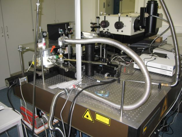
Micro Photoluminescence Spectroscopy
- high resolution 1m-Czerny-Turner Monochromator
- nitrogen cooled CCD-Camera (deep depletion, anti-etaloning)
- Cryostat cooled with liquid helium, Temperature Range: 3,5K-475K
- high resolution Linear Stages with 0,1µm position control
- microscope objective with 0,7µm resolution power
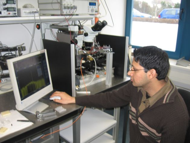
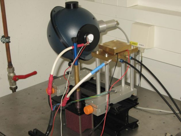
Laserdiode Characterization ( pulsed )
- Driver current up to 2A
- 500ns puls duration, 1ms puls distance
- Temperature control from -10°C up to 150°C
- Ultrafast InGaAs- und Si-photodiodes for detection
- Farfieldmeasurement for x- und y-Axis
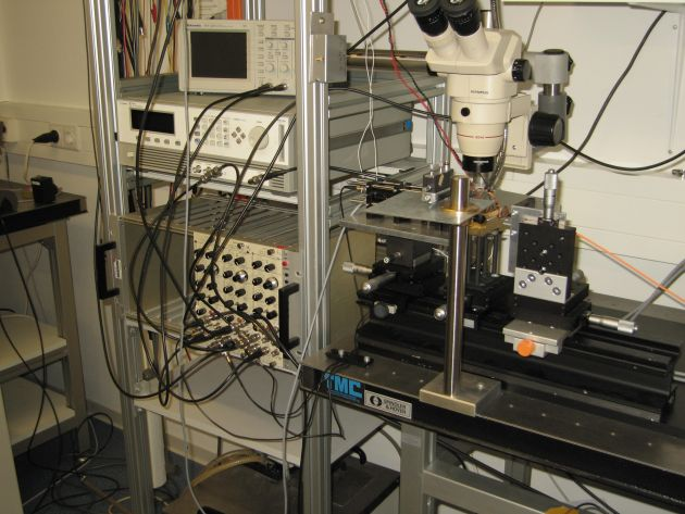
Laserdiode Characterization ( cw )
- Driver current up to 500mA, with 10µA resolution
- Measurements of Multisectionlasers (3 Needles)
- Temperature control from -10°C up to 150°C
Laserdiode Characterization ( high power cw )
- Driver current up to 40A, 10mA resolution
- Complete laser diode characterization Io,Vf and Po
- Temperature control from -50°C up to 150°C, accuracy of +/-0,1°C
- Heat sink integrated
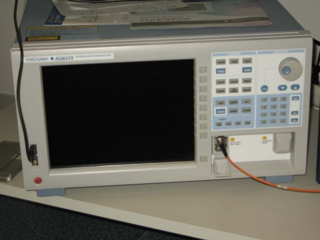
Optical Spectrum Analyser
- Wavelength sensitivity range: 600nm - 1700nm
- High resolution of 0,02nm
- Suited for DWDM-Networkanalysis
- Extensive Analysis- and Fittingfunctions (Power,WDM,SMSR,etc.)
- 7 independent measurement tracks
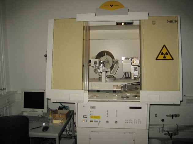
Phillips PW 3710 MPD X-ray diffractometer
- High resolution (thickness, strain, dislocations)
- 3-Axes Geometry
- suited also for powder
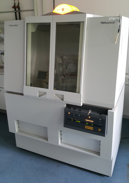
PANalytical X’Pert Pro MRD
-Offene Eulerwiege mit XYZ-Probentisch
-Rocking curve-/ Triple Axis-Sekundäroptik
-Hochauflösungs- , Textur-, Spannungs- und Reflektivitätsmessungen (Auflösung von 0,0001°)
-Hochauflösendes Mapping im reziproken Raum, Akzeptanzwinkel 12‘‘
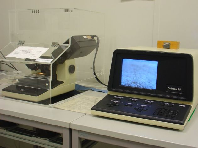
Sloan Dektak IIA Profilometer
- 20nm resolution
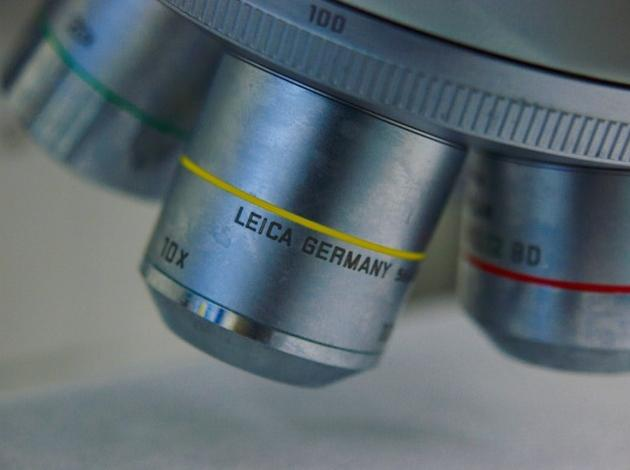
Leica DMR Microscope
- up to 1000x Magnification
- Contrast methods: bright field, dark field, differential interference contrast
- Impinging light and transmitted light
Plasmos SD-2100 Ellipsometer
Monitoring of film thickness
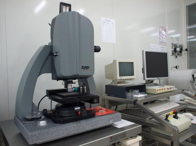
Zygo New View 5000 White Light Interferometer
- Vertical resolution down to 0.1nm
- Objectives: 5x Michelson, 50x Mirau
- xy-motordesk for stitching
- Extended vertical scan length up to 20mm
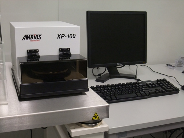
Ambios Technology surface profilometer XP-100
- 3 nm measurements accuracy
- 0,03-10 mg Stylus-compression force
- 1,2 mm. max range of measurement in the z-direction
- analysis of step height, layer thickness, roughness, waviness, thin-layer stress