Quantum Coins and Nano Sensors
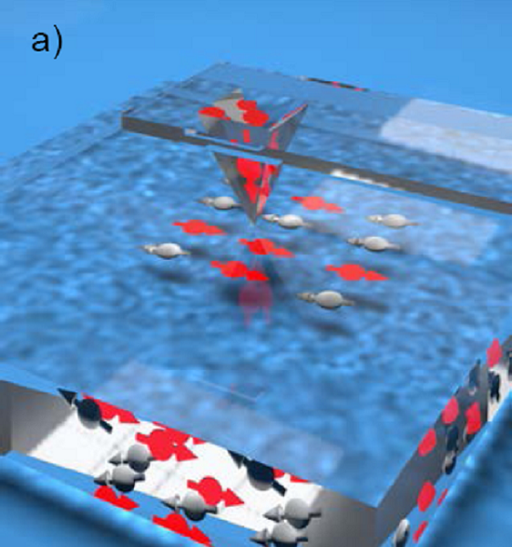
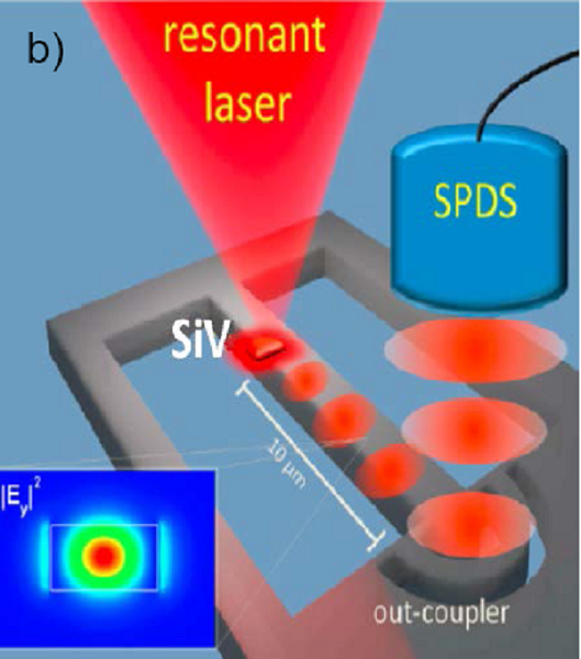
We aim at fabrication and testing of devices from polycrystalline diamond targeting two main applications: The development of dedicated quantum memory for quantum coins implementation and quantum sensing of magnetic fields. With the deterministic nano-implantation system we will integrate nuclear spins next to color centers such that long lived quantum states can be stored. Low-cost polycrystalline diamond fabrication expertise and nano-structuring facilities allow us to tackle the full production chain of the final device. The theory partners in Kassel will enhance the protection of the quantum coin by identifying decoherence-free subspaces (DFS). This improves the quality of the quantum coin but also allows for the realization of sensors that are protected against environmental noise with increased sensitivity to signals outside of the DFS, providing the design principle for sensitive and selective nano-gradient sensors. The theory partner in Erlangen will focus on quantum and classical protocols to implement a robust quantum device. They will develop protocols based on redundancy and error correction specifically optimized for this application.
Project Partners
- Prof. Kilian Singer, Institute of Physics, Light-Matter Interactions, University of Kassel
- Prof. Ferdinand Schmidt-Kaler, Institute of Physics, University of Mainz
- Prof. Christiane Koch, Institute of Physics, Theoretical Physics, University of Kassel
- Prof. Eric Lutz, Institute of Theoretical Physics, University of Erlangen-Nürnberg
Picture gallery