This page contains automatically translated content.
Scientist involved in major project on quantum communication
 Image: Paavo Blafield.
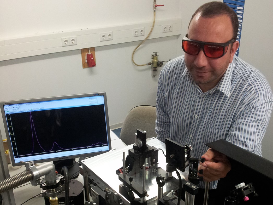 Image: Paavo Blafield.
Quantum technology is based on complex physical laws; for example, certain information carriers assume different states simultaneously or can be entangled with each other at a distance. Quantum communication uses this to transport information that cannot be copied or read unnoticed. However, when it comes to transmitting quantum information using light particles over fiber optic networks, the technology still faces very practical limitations. Due to line losses, the transmission distance has so far been limited to less than 100 kilometers. So-called quantum repeaters are now to significantly increase the range; similar to repeaters in conventional communications technology, they are to pick up signals and send them further in amplified form.
The German Federal Ministry of Education and Research is now funding a large-scale joint project involving 24 partners with almost 15 million euros to research and develop different variants of repeaters: Conceivable are repeaters based either on quantum dots, on diamond color centers or on a combination of atomic and ionic systems. In the Q.Link.X project, not only individual components of a quantum repeater are being developed for the first time, but complete communication links.
In the process, a Kassel research group led by Priv.-Doz. Dr. Mohamed Benyoucef from the Institute of Nanostructure Technology and Analytics (INA) is developing quantum dots on the novel basis of an indium-phosphorus compound. They are designed to emit single and entangled photons specifically in an area of fiber optic networks that is particularly slow to transmit, thus greatly reducing losses. Quantum dots are tiny nanoscale crystals, usually made of semiconductor materials, with special physical properties. They are used in quantum technology, for example, as single photon sources.
In a second part project, a group led by apl. Prof. Dr. Cyril Popov, also from INA, is developing specific diamond-based photonic structures using electron beam lithography and reactive ion etching. These include nanocolumns, photonic crystals and waveguides. The structures will be coupled with various diamond color centers to increase photon collection efficiency.
InP-based quantum dot structures subproject.
Many applications of quantum information technology rely on the transmission of information using single photons. The transport of these photons over long distances in optical fiber networks requires single photon sources as well as entangled photon pairs with compatible wavelengths in the telecom C-band region of 1.55 µm, where the attenuation of optical fibers is minimal. Quantum dots (QPcts) based on indium phosphide (InP) are a possible candidate to achieve the targeted telecom window at 1.55 µm. Self-assembled InAs QPkte are grown on InP substrates using solid-source molecular beam epitaxy. QPcts are small objects, tens of nanometers in size, composed of thousands of atoms and are often referred to as "artificial atoms" because they locally have individual charges in discrete energy states, analogous to the energy levels of the orbitals of natural atoms. The goal of the InP-based quantum dot structures subproject of the group of Priv.-Doz. Dr. Mohamed Benyoucef, Institute of Nanostructure Technology and Analytics (INA) at the University of Kassel, is to develop materials and platforms suitable for the use of quantum repeater protocols for secure quantum information processing and transmission. The group is developing quantum dots based on InP that emit single and entangled photons specifically at 1.55 µm (telecom C-band). Losses are to be greatly reduced in the process. In particular, the focus of the subproject is on the structural optimization of the emission properties via epitaxial growth as well as on an integration of quantum emitters in more complex emitter structures e.g. microcavities for strong light emission and pin-/ Schottky diode structures for spin manipulation; here, doped QPcts and quantum dot molecules with controlled doping levels shall be used as chargeable structures.
Subproject diamond-based photonic structures
Color centers (single atomic vacancies) in diamonds can act as long-lived quantum memories - due to the advantageous long coherence times of electron and nuclear spins in combination with efficient optical transitions. For the transfer of quantum information, photons serve as an interface to the spins of the color centers. This interface is ensured by a combination of microwave and optical transitions for the so-called nitrogen defect sites (NV centers) or by direct optical spin control for the so-called silicon defect sites (SiV centers). The diamond solid-state platform offers integration "on-chip", i.e. the structures are embedded in the diamond membrane, with photonic elements to selectively enhance the spin-light interaction. The goal of the diamond subproject of the group of apl. Prof. Dr. Cyril Popov, Institute of Nanostructure Technology and Analytics (INA) of the University of Kassel, is the realization of diamond-based photonic structures (nanocolumns, photonic crystals, waveguides) by means of electron beam lithography and reactive ion etching. All the mentioned structures are coupled with color centers (NV, SiV) to increase the photon collection efficiency. To achieve this, implantation masks are developed for deterministic implantation of nitrogen or silicon and the resulting generation of color centers. Coherent manipulation and efficient spin state readout will be enabled by integrating the photonic structures with metal electrodes and antennas. The structures will serve as spin-photon interfaces as well as components of quantum memories for studies at Q.Link.X project partners.
Participating institutions
The following partners are involved in the project: Rheinische Friedrich-Wilhelms-Universität Bonn, Technische Universität München, Technische Universität Dortmund, HighFinesse Laser and Electronic Systems GmbH, Fraunhofer Heinrich Hertz Institute Berlin, Technische Universität Berlin, Universität Stuttgart, Universität Paderborn, Saarland University, Freie Universität Berlin, Leibniz Institute for Solid State and Materials Research Dresden, Ruhr University Bochum, Swabian Instruments GmbH, Leibniz University Hannover, Max Planck Institute of Quantum Optics (Garching), Julius Maximilian University Würzburg, University of Bremen, Heinrich Heine University Düsseldorf, University of Ulm, Humboldt University Berlin, University of Kassel, Johannes Gutenberg University Mainz, Karlsruhe Institute of Technology, and Ludwig Maximilian University Munich.
Part of this text is based on a report from the University of Bonn on the same topic: https://idw-online.de/de/news703142
Further information:
https://www.forschung-it-sicherheit-kommunikationssysteme.de/projekte/q-link.x
Contact:
Sebastian Mense
University of Kassel
Communications, Press and Public Relations
Tel.: +49 561 804-1961
E-mail: presse[at]uni-kassel[dot]de
www.uni-kassel.de